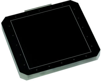
For a manufacturer of X-ray detectors in the medical industry, we have created an advanced modular image storage system with an FPGA and DDR3 chips.
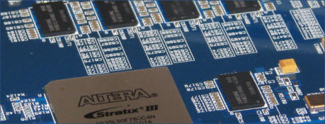
A lot of X-ray detectors are equipped with a Gig-E vision interface, a standard created in 2006 based on Gigabit Ethernet. Over the years image sensor resolutions have increased in such a way that the frame rate is limited when using this interface. To overcome this problem the sensor data has to be read out fast and transferred to the DDR3 memory. Then, the images can be read from DDR3 at lower speed and transmitted over the Gig-E interface. A challenging requirement was the ability to store 500 high resolution images in memory.The customer already defined the hardware platform. We defined the internal FPGA architecture and created a bandwidth calculation model to find out how many DDR3 chips where needed to fulfill the frame rate and storage capacity specifications. The latter made clear that the total DDR3 memory size had to be 2 Gigabyte.DDR3 chips are designed to operate in a fly-by topology. The DDR3 controller in the FPGA therefore needs to support read and write leveling for maximum performance. To enable reading and writing streaming and random images to and from the DDR3 memory, a custom file system has been developed. This file system includes adding time stamps, sequence numbers and other settings to each image. And to be able to verify the integrity of each image a CRC is added.The block diagram shows the system architecture of the image processing subsystem and its related components. Central part is the packing/unpacking core. Streaming image data comes in here and is packed to the file format and written to the DDR3 controller via the Avalon bus. When the Gig-E transmitter (not shown here) is ready to receive data, the unpacker reads the images out of memory and reformats the data to the original image stream.The NiosII host processor controls the packing/unpacking core via the register file block. This block holds all the register settings that the processing core needs. Registers are set by the NiosII via the Avalon bus. The register file is generated with our register builder software. To mimic the behavior the DDR3 controller and DDR3 chips a simulation model has been developed and used in a test bench. This test bench sets all the relevant registers and contains a dummy image stream data generator with pseudo-random data and a verification unit to check the result.For hardware debugging of the total subsystem a dummy image stream generator (inside the FPGA, not shown here) can be connected to the core. With a command line utility the NiosII can enable the dummy data and start and stop capturing images to memory and reading out image data. When reading images from memory CRC errors are logged automatically by the core. This logging data is available to the host and is used for system debugging.The system is delivered to our customer and is in full production.